Chipmakers want every part of the wafer to produce, or yield, good die. Advances in process technologies over the years have just about made this a reality, even as feature dimensions continue to shrink and devices grow ever more complex. Now, the last frontier is improving yields at the edge of the wafer – the outer 10 mm or so – where chemical, physical, and even thermal discontinuities are simply much harder to control. Complicating matters, current strategies used to manage these edge issues involve tradeoffs between yield and manufacturing costs that result in less than ideal fab economics. At Lam, our technologists have been working on solutions to this challenge, and today, we released the new Corvus™ edge control technology for our Kiyo® conductor etch products to address these very issues and enhance edge yield.
Edge Challenges
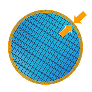
Taking a closer look at the wafer’s edge, where up to ~10% of the die may be located, there are several issues at play that can impact yield. In all plasma etch reactors, the abrupt end of the wafer surface creates inherent electrical discontinuities at the edge region, forming voltage gradients that bend the plasma sheath. This, in turn, changes the direction of the plasma’s components (ions and neutrals), which impacts etch results and causes unwanted variability. In the case of 3D NAND devices, for example, this change in the plasma conditions at the wafer’s edge can cause tilted etch profiles or prevent features from being completely etched. In addition to affecting tilt angle, these edge effects can result in non-uniform critical dimensions (CDs) or changes in local overlay metrics.

Another challenge is that process drift creates CD uniformity and selectivity problems over time. As a way to manage this, chipmakers often add more chamber wet cleans to restore the equipment to a standard condition. However, this approach significantly reduces productivity because the chamber is not available for processing wafers during this maintenance. In addition, as process margins get tighter, more frequent wet cleans are required, which increases operational costs.
Corvus Solution
Lam’s new Corvus technology provides a novel capability to smooth out extreme edge discontinuities and enhance edge performance. It offers the ability to tune the plasma sheath at the edge to produce a constant, user-defined etch rate and ion angle. For example, etch rate can be tuned to be faster or slower at the edge relative to the rate over the rest of the wafer. With 3D NAND applications, Corvus technology has demonstrated the ability to minimize plasma sheath drift, preventing detrimental feature tilting at the wafer’s edge. Tuning to within 1.5 mm of the edge, the new technology can correct for inherent process variation in the edge region as well as for incoming film variations to optimize die yield. Furthermore, with Corvus, every wafer sees the same edge conditions for optimal yield, eliminating previously seen systematic wafer-to-wafer yield variability.

Corvus technology not only improves across-wafer uniformity, it also greatly reduces wafer-to-wafer and chamber-to-chamber variability and eliminates the historical tradeoffs among yield, operational flexibility, and cost. Customers have reported die yield improvements of 0.5-2% per wafer, which can be a significant advantage – especially when you consider how many thousands of wafers chipmakers process every day. Additionally, Corvus has demonstrated the ability to provide higher and more consistent yield over a longer period. It also greatly enhances productivity and lowers overall fab operating costs for high-volume manufacturing by requiring fewer chamber wet cleans. The new technology is being used for advanced patterning, mask open, and other challenging conductor etch applications where reducing variation in CD, profile, or selectivity and improving productivity helps enable continued scaling.
The new capability provided by Corvus complements Lam’s Hydra® technology, which enables fine tuning of within-wafer uniformity and actively compensates for incoming variation. Together, these advanced process control technologies are reducing variability across the entire wafer surface, improving yield, and enabling the production of next-generation logic and memory devices.