Since its introduction in the 1980s, NAND flash memory has radically changed how we store our digital data. Remember ordering duplicate photos when getting camera film developed or burning your music playlist to an audio CD? Those approaches to data storage have been replaced by memory cards, USB drives, and solid state drives that seem to increase in capacity every few months. The enabling technology behind these products is NAND flash memory, which is named after the “not-AND” logic gate that the individual memory units resemble. NAND-based products process data quickly, so it’s no surprise they have found their way into devices we use every day. Read on to learn more about this transformative memory technology and its latest inflection, 3D NAND.
Conventional NAND Scaling Only Goes So Far
NAND products store information in structures called “cells,” which are arranged in rows and columns. These cell arrays are conventionally manufactured in the wafer plane (referred to as planar NAND). Historically, memory density was increased by shrinking cell size and spacing. For example, if the cell size and spacing is reduced to half of the original size, then four times as many structures can fit into the same area. Once NAND cell dimensions shrink to a certain size, however, further reductions are hindered by technological barriers. Continued scaling using traditional lithography-intensive patterning also becomes extremely costly. As a result, different design concepts and manufacturing methods are needed to continue increasing memory density.

There are three images showing smaller individual cell size results in more cells per unit area. Image one shows a 120nm x 120nm box with four cells. Image two shows a 60nm x 60 nm box with 16 cells. Image three shows 30nm x 30nm box with 64 cells.
NAND Moves to the Next Dimension
Just like in real estate, when you can’t keep building out, you build up – and 3D NAND structures are the skyscrapers of the memory world. Instead of creating a string of memory cells that lies in the wafer plane, 3D NAND devices build the string vertically. Creating these three-dimensional structures requires developing new fabrication methods, which rely heavily on deposition and etch processes.
The manufacturing process starts with depositing multiple alternating layers of materials, such as oxide and nitride films. Long and narrow vertical holes are then etched through this film stack to form the channels. Other critical steps in memory cell formation include staircase etch of the dielectric film pairs and metal fill of the contacts and bit lines. In the case of replacement-gate schemes, additional critical steps such as the lateral (or horizontal) metal word line fill are needed.

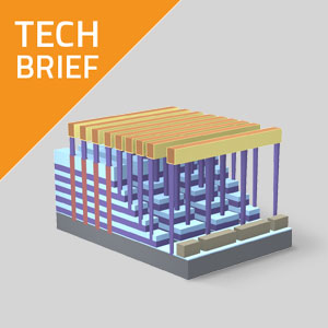
The image shows key process steps in 3D NAND memory cell formation. There is a cutaway rendering of such a cell showing:
- Channel: Hardmask open
- Single memory cell
- Stack: alternating film deposition
- Channel: High aspect ratio etch
- Word line: Metal fill
- Stair: Staircase etch
- Contact: Metal fill
- Bit line: Metal fill
Challenges in Creating 3D NAND Structures
Building in three dimensions means that process variability must be controlled on both the horizontal and vertical planes. How big a challenge is this? Let’s look in a little more detail at a few of the critical steps for memory cell formation.
Creating the film stack requires depositing multiple, thin layers of oxide/nitride (ONON) or oxide/polysilicon (OPOP). Each layer must be highly uniform and extremely smooth and have good adhesion to the one below. These challenges grow as more layers are added. Any defect or small variation in film thickness can result in a large deviation at the top of the stack, which can lead to poor device performance. In addition, film stress management becomes critical and more challenging with increasing layers, as does the need for high productivity to achieve cost-effective production.
The channel hole etch is one of the most challenging processes. In planar NAND, holes have aspect ratios of ~10:1, or roughly 10 times taller than wide. However, the aspect ratios for 3D NAND holes are much higher, more than 40:1. Maintaining a uniform hole diameter from the top to the bottom of the film stack is tricky since tall, narrow features tend to distort. Tight control is needed to minimize bowing and twisting of the channel, which could lead to shorts or interference between neighboring memory strings.
Metal fill of the word line is another critical step for replacement-gate schemes. To reduce signal delay, the word line is backfilled with a conductive material such as tungsten after the sacrificial layers (such as nitride in ONON stacks) have been removed. This step is particularly challenging because of the complex geometries involved. The lateral deposition process has to completely fill narrow, horizontal features without leaving any voids in the metal for each replacement-layer in the stack.

The image shows 3D NAND Manufacturing Challenges. There are three, depicted in three columns:
1) Film stack deposition - Increasing number of pairs requires high productivity; Impact of defects are magnified; Non-uniform layers
2) Channel etch - Bowing; Selectivity to hardmask; CD variation at top vs. bottom; Twisting; Incomplete etch
3) Word line fill - Lateral fill required; voids in tungsten
How High Will These Memory Skyscrapers Go?
These manufacturing challenges become even more difficult as the 3D NAND stack heights scale from ~30-40 layers today to ~60 or more layers in the future – all in pursuit of higher memory density. Fortunately, advanced deposition and etch systems are making high-volume production of 3D NAND devices a reality, delivering high productivity while minimizing variability.
As demand for greater amounts of digital information grows, 3D NAND and other advanced memory technologies will continue to play a key role in providing higher density storage solutions. We may soon be carrying around devices with terabytes or even petabytes of memory – we’ll never fill that up, right?