We often hear that advanced chips contain billions of transistors – an incredible, mind-blowing fact to be sure – but did you know that large-scale integrated chips (that are the size of a fingernail) can contain ~30 miles of interconnect “wires” in stacked levels? These wires function like highways or pipelines to transport electrons, connect transistors and other components to each other, and make them functional. And just as the speed you can drive your sports car depends (at least in part) on how clogged the freeway is, chip performance depends on the ability to move signals and power through these ultra-tiny wires. In fact, as the shrinking of feature dimensions (scaling) has continued, interconnects are now becoming the speed bottleneck in today’s most advanced chips. So, let’s spend a little time learning about them.
Interconnect Layers
During the first portion of chip-making (or front-end-of-line), the individual components (transistors, capacitors, etc.) are fabricated on the wafer. In the back-end-of-line, these components are connected to each other to distribute signals, as well as power and ground. There simply isn’t room on the chip surface to create all those connections in a single layer, so chip manufacturers build vertical levels of interconnects. While simpler integrated circuits (ICs) may have just a few metal layers, complex ICs can have ten or more layers of wiring.
Interconnects close to the transistors need to be small, as they attach/join to the components that are themselves very small and often closely packed together. These lower-level lines – called local interconnects – are usually thin and short in length. Global interconnects are higher up in the structure; they travel between different blocks of the circuit and are thus typically thick, long, and widely separated. Connections between interconnect levels, called vias, allow signals and power to be transmitted from one layer to the next.

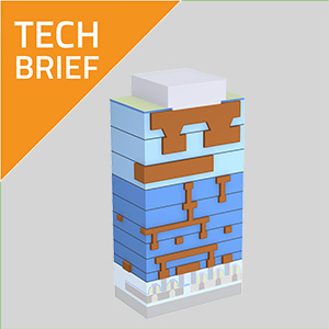
On the left is a cutaway of a chip in which everything has been removed except for Metal Lines, which are used to connect integrated circuits. At the top is Level 2 (metal line) with a vertical Via connecting it to Level 1 (metal line). Level 1 is then connected to the chip (Device Transistors) by two Vias.
On the right is a filled in integrated circuit showing the metal lines. The Global interconnects are stacked on top of the Local interconnects.
Interconnect Materials
For decades, aluminum interconnects were the industry standard. To create these interconnects, a layer of aluminum was deposited. Then, the metal was patterned and etched, and insulating material was deposited to separate the conducting lines. In the late 1990s, chipmakers switched to copper, which conducts electricity better than aluminum – somewhat similar to how a copper-bottomed frying pan heats up faster than an all-aluminum pan.
Higher conductivity lines improved overall IC performance. In addition, copper lines could be made smaller, keeping pace with transistor size scaling. Copper wiring is also more durable and reliable. However, creating copper interconnects is much more complex, and a whole new manufacturing scheme had to be developed for this technology inflection. The copper interconnect process starts with deposition of an insulating (dielectric) material, for example silicon dioxide, followed by the creation of trenches. The trenches are then filled with copper (using chemical/electroplating technologies), and the excess is removed to form a flat surface for subsequent processing.

The RC Challenge
Over the years, transistors have decreased dramatically in size. As transistors have gotten smaller and smaller, interconnects also have had to scale in size. Today, we’re at the point where conventional copper interconnects are facing a significant roadblock to further scaling, and that roadblock is known as the RC challenge. Let’s pause to define these two variables.
The electrical resistance (R) of a material describes how difficult it is to move electrical current through a particular cross-section of that material, which is a function of the orientation and proximity of the material’s atoms. Capacitance (C) refers to a material’s ability to store electrical charge. The product of resistance and capacitance (RC) needs to be low to create fast chips since device speed is inversely proportional to RC (lower RC = faster devices).
Looking at the “R” side of this challenge, higher-resistance lines carry less current, which slows device speed. This is because higher resistance reduces electron flow, so it takes longer to build up the minimum charge (number of electrons) or “threshold voltage” at a transistor’s “gate” to turn it on. While transistor speed continues to improve with scaling (reducing the distance electrons must travel), the challenge for interconnect scaling is to not become a bottleneck and lose that performance improvement by slowing the flow of electrons between transistors.

High Resistance With Smaller Line Width
There is a chart on the left. The Y axis is Copper Line Resistance (arb) and the X axis is Line Width (nm), going from 0 to 60. A line starts really high up the chart ~12 nm and swoops down and to the right to very low on the chart at ~52nm width.
The images on the right show the difference between a Wide copper core and a narrow copper core sitting in Dielectric.
On the “C” side, capacitance is a function of the insulating dielectric material around the metal lines and the distance between them. Higher capacitance slows electrons and can create unwanted “cross talk,” where the signal (voltage change) in one metal line influences the signal in a neighboring line and causes the device to malfunction. In addition to maintaining a suitable distance between lines, the development of “low-k” dielectric materials (capacitance is a function of a material’s “k value”) has significantly lowered capacitance. Today’s dielectric materials average around k = 2.5, compared with k = 4.2 for pure silicon dioxide. Various methods exist to achieve lower values; however, the resulting ultra-low-k films become increasingly fragile as the k value decreases, posing additional challenges for use in manufacturing.
Scaling Solutions and Future Directions
To address these issues for further scaling, the industry continues to identify ways to manage RC, particularly focusing on the metals involved. Copper has been successfully used for multiple device generations, so the industry is investing significant effort in developing new approaches to extend its use. Creating copper lines involves a series of layers – typically a tantalum nitride barrier (prevents metal diffusion into the dielectric), a tantalum liner (improves barrier adherence to the metal), a copper seed layer (initiates the metal fill/plating), and finally, the bulk (core conducting) copper metal. A key area of development focus is identifying strategies for improving the barrier/liner/seed layers to lower overall resistance and enable smaller lines by creating “space” for the bulk copper fill.
One strategy is to make the high-resistance barrier and liner thinner. However, opportunity for further thinning of these layers is limited. Both need to be continuous (no gaps or voids in the film) in order to achieve good reliability performance. This requires a minimum thickness of about 1.5 nm to 2 nm for each layer, which leads to a combined thickness of 3-4 nm on both sides of the trench structures.
A potential alternative being studied is a new type of “self-forming” barrier that reacts with and forms on the dielectric surface adjacent to the copper line, which allows more room for copper. Also, new liners made of cobalt and ruthenium are being developed to replace tantalum. They adhere better to the copper seed, enabling it to be more conformal (eliminating voids) and thinner. Already, new technologies are in place to achieve void-free copper fill of small trenches. Around the 5 nm technology node, however, copper as the primary conducting metal will ultimately have to be replaced with a conducting material that does not require a barrier for these ultra-thin lines.

While much attention is placed on the metals, there’s also some investigation into improvements on the dielectric side. Here, the holy grail is to reduce the dielectric constant as much as possible, the ultimate being k = 1, which is air. Indeed, novel developments using “air gaps” have been used, but both fabrication and production cost challenges are significant. Thus, many of the ideas being explored for interconnect scaling involve the development of new metals, designs, and processes – and those new technologies that are in the “pipeline” are sure to make ever smaller, faster connections a reality.