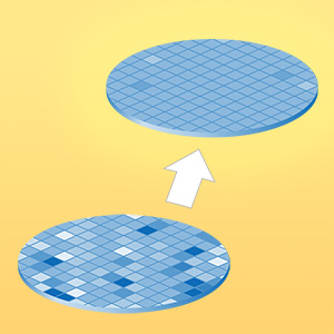
Multiple patterning continues to be an important technique for enabling pitch shrinking in advanced chip designs. However, as the number of steps grows, managing process variation is a key concern. In part two of a two-part series published in EE Times India, Rick Gottscho, Lam’s corporate chief technology officer, identifies primary sources of variation and techniques being developed to address them.
Multiple patterning, a method for increasing IC feature density beyond the limits of conventional lithography capability, has emerged as an important technology for manufacturing advanced chips (see Enabling advanced ICs with multiple patterning). This technique has proven to be an effective method for pitch shrinking with two- and four-fold reductions now standard in high-volume production. However, as the number of process steps increases, managing variation becomes more critical.
For example, in the self-aligned quadruple patterning approach, critical dimension (CD) is impacted by lithography, deposition, etch and clean, potentially resulting in three different contributions to CD variation of the space between lines. Stringent control is required at each process step of the multiple patterning scheme to ensure consistent line placement required for device scaling.
CD Uniformity
The maximum allowable variation in patterning is quantified as “edge placement error.” Generally, this should be less than 30% of the minimum feature pitch and includes all sources of variation. To meet this requirement at the 5 nm node, variation across the wafer must be less than 0.5 nm.
Control of plasma etch across the wafer is critical to the overall chain of process uniformity management efforts. Key challenges include managing inherent thermal, chemical, and electrical discontinuities due to the finite wafer size, as well as developing tuning methods that can provide independent control of process parameters.
Initial innovations to reduce variability focused primarily on tuning the plasma chemistry across the wafer, such as injecting reactant gases from multiple locations and adding tuning gases in specific areas to control the reactant ratio at the wafer edge versus the center. This enabled a significant step forward in controlling the chemistry and convective transport factors that impact variability. Process control methods evolved with multiple injection locations—including at the wafer edge—to significantly improve the spatial resolution of chemistry control.
Continue reading at the EE Times India website.
