Silicon chip manufacturing has always included etching as a critical processing step. But, increasingly, extremely high-aspect-ratio etching has been needed for 3D flash and DRAM chips, which have revolutionized the capabilities of everyday electronics such as smartphones, laptop computers, and the many other electronic devices that we use on a daily basis. This has increased the demands on etching equipment, and Lam’s high-performance etch tools have been critical enablers of the success of these processes.
Those tools involve plasma etching, and the equipment has a very carefully constructed chamber in which the etch reactions take place. The parts that are assembled together to create that chamber must be able to withstand the extremely harsh environment of an active plasma. Historically, those parts were made of ceramics. They were robust in the face of the most aggressive etch processes, but they had poor defect performance. In addition, electrical differences between the silicon wafers being etched and the ceramic components made the plasma hard to control near the edges of the wafer, hurting yield.
In contrast to those ceramics, silicon provides a defect-free material that has the same electrical properties as the wafers. This allows for fine control of the plasma even near the edge of the wafer, improving yields.
Silicon Parts – Different from Silicon Wafers
But making etch chamber parts out of silicon is not the same as making silicon wafers. The challenges it presents – and the expertise needed to address the challenges – are very different. Silicon parts have complex 3D features that include high-aspect-ratio holes, threaded screw holes, and slots. And silicon is a notoriously brittle material, so truly innovative techniques are required for machining those features and for finishing the surfaces.
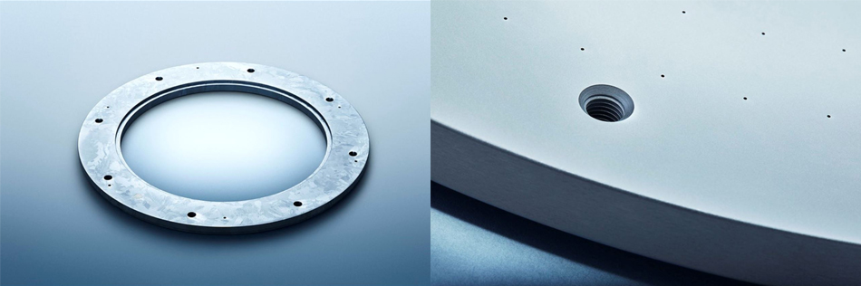
Etch chamber parts also drive different bulk silicon material requirements than wafer manufacturing. The bulk defectivity of silicon ingots intended for wafers is not so critical, since the processing and electronic activity occur on the surface. Any bulk defects remain hidden within the wafer. By contrast, silicon parts must be made from ingots with very low bulk defectivity. That’s because the parts will have millimeters of material etched away during the most aggressive plasma processes, and that will eventually expose those internal defects. They can reduce the yield of the wafers being etched.
The ingots themselves are much larger than the ones used for wafers, and their size will vary according to the dimensions of the chambers and the specific parts being built. That means that the tools used to slice the ingots and polish surfaces are non-standard.
Silicon Parts – An Important Lam Business
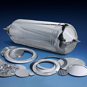
Lam creates silicon parts in its Silfex subsidiary, with product specifications superior to those of competing parts. Lam makes both the etch equipment and the parts used inside the equipment. This means that the team creating the silicon parts can confer with the team creating the etch tools, providing a tight communication loop for optimizing the performance of the parts.
Part designs are carefully tailored to maximize the lifetime of the part during plasma processing. Customers can both reduce their maintenance costs and increase the uptime of their etch equipment, contributing to increased manufacturing profitability.
Silicon parts are an important business for Lam. By driving innovation in the materials used for their etch equipment, Lam can offer etch tools for demanding high-aspect-ratio applications with superior performance and affordable cost of ownership. Excellence in the parts market is one of the many factors keeping Lam in a leadership position.