Lam’s newest product in its line of GAMMA® dry photoresist strip systems, brings the performance of the GAMMA® GxT® 300 mm to 200 mm wafer processing. The GAMMA GxT has been specifically designed for the specialty technologies market, bringing exceptional reliability, productivity, and flexibility to these applications.
Photoresist strip has historically been a low technology process, but has become increasingly more complex with 3D structures, double patterning, multiple layer masks, and high dose implant strip (HDIS) applications. Many requirements have been or are being actively addressed for advanced memory and logic nodes at the 300 mm wafer size. However, those challenges at 200 mm for specialty technologies — including RF filters, power, read heads, and digital printing — are often ignored by the leading equipment OEMs or manufacturers. The technology differentiators at 300 mm are not necessarily common to 200 mm, where low temperature processing, the ability to handle both thick and thin resists, alternate materials for strip, and multiple substrate type handling dominate.

Strip applications are needed throughout the process flow. Each application presents its own set of needs and requires the capability to handle multiple applications in one system.

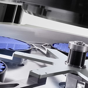
The GAMMA GxT is an industry leading multi-station and multi-process solution for advanced strip applications with high reliability and productivity. Multiple process steps can be performed with maximum flexibility and productivity on the same platform, enabled by Multi-Station Sequential Processing (MSSP) architecture. This allows for independent control of temperature, RF power, and chemistry. The system provides residue-free results with high throughput and low defectivity performance for both bulk and implant strip applications due to enhanced source technology combined with faster wafer heating.
A wide array of chemistries are available with the flexible gas box:
- Traditional O2/N2 for bulk strip from thin DUV photoresist layers to >10 µm i-line and thick amorphous carbon ash
- CF4 HDIS and polymer removal
- and H2 or forming gas (FG) for HDIS and low silicon or residue removal
Low temperature capability down to 110°C for descum and a wide temperature window for standard processing, facilitates a broad range of specialty technology processes for semiconductor and advanced hard-drive applications. Industry leading mechanical throughput up to 350 wph with a small footprint provide exceptional productivity.
Lam’s 200 mm GAMMA GxT has been specifically designed to address the challenges of the specialty technologies market, bringing exceptional reliability, productivity, and flexibility to these applications.