Did you know that different patterns require different types of multiple patterning? Today’s advanced chips are more complex than ever before, with transistors and other structures that are smaller and more densely packed. To create those tiny features, chipmakers have developed multiple multiple patterning strategies that enable much finer dimensions than current lithography can achieve.
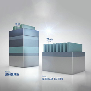
Multiple patterning techniques such as litho-etch-litho-etch (LELE) and self-aligned patterning are used today to create holes, 2D lines, and uni-directional (1D) lines. The litho-etch method splits dense layouts into less-dense parts, which are formed by alternating lithography and etch steps. Self-aligned double-patterning (SADP) and self-aligned quadruple patterning (SAQP) – sometimes referred to as spacer-based patterning – rely heavily on deposition and etch processes to achieve the final pattern.

Three icons showing three types of patterning: 1) Holes (a bunch of holes), 2) 2D Lines (lines going in different directions) and 3) Uni-Directional (1D) Lines (with many lines going in the same direction)
These multiple patterning schemes have enabled pitch shrink far below the resolution limit of conventional lithography and will continue to be used with future lithography capabilities. Watch our latest video to see how some of these patterning techniques work and their applications.
Want to learn more? Here are some additional resources: