Atomic layer etching (ALE) is one of the chipmaking processes that makes our data-driven world possible. After being confined to the laboratory for decades, ALE has awakened to become the most advanced etching technique in production today. It delivers the incredible control needed to create advanced logic and memory device structures, which in turn, enable the smaller, faster, and better performing electronic devices we use every day.
An article by Lam technologists on this etching technique was recently published in a prestigious technical journal. The perspective first discusses various etch mechanisms, then examines the ALE behavior of a variety of elemental materials and binary compounds. Two benefits, improved material selectivity and smoother surfaces, are also covered. The abstract is included below.
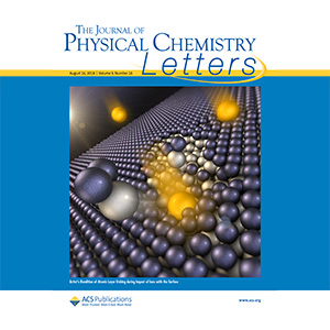
Atomic Layer Etching: Rethinking the Art of Etch
Keren J. Kanarik, Samantha Tan, and Richard A. Gottscho
Atomic layer etching (ALE) is the most advanced etching technique in production today. In this Perspective, we describe ALE in comparison to long-standing conventional etching techniques, relating it to the underlying principles behind the ancient art of etching. Once considered too slow, we show how leveraging plasma has made ALE a thousand times faster than earlier approaches. While Si is the case study ALE material, prospects are better for strongly bound materials such as C, Ta, W, and Ru. Among the ALE advantages discussed, we introduce an ALE benefit with potentially broad application—the ALE smoothing effect—in which the surface flattens. Finally, regarding its well-established counterpart of atomic layer deposition (ALD), we discuss the combination of ALE and ALD in tackling real world challenges at sub-10 nm technology nodes.
Read the full article at: J. Phys. Chem. Lett., 2018, 9, pp 4814–4821