Perspectives on Advanced Interconnect Developments

Industry experts came together recently to discuss some of the critical challenges facing interconnect scaling. As the number of transistors on advanced chips continues to increase, fabricating the tiny wires that connect them becomes more complex, raising several questions. How will we fabricate these dense, complicated interconnects? Will new materials be needed below the 10 nm technology node? Are there paths to extending or replacing current technologies? These were among the topics covered at Lam’s Technology Seminar held during the 2016 International Interconnect Technology Conference (IITC) and Advanced Metallization Conference (AMC) joint conference in San Jose. In case you missed it, we’ve put together a summary of some of the key points shared at our evening event.
Innovations May Extend Current Technologies
Today’s advanced chip performance is limited by the speed at which signals are transmitted through the connecting wires. It’s no surprise, then, that one of the big topics of discussion was the need to reduce interconnect delay. As device dimensions shrink, resistivity of the current-carrying metal increases rapidly due to electron scattering. The lack of liner/barrier and seed thickness scaling also contributes to higher resistance since there is less volume available for the bulk metal, which today is copper and tungsten.
The industry is searching for alternate materials and integration schemes to overcome the resistance-capacitance (RC) challenge. During his seminar presentation, Lam’s Chief Technology Officer Dave Hemker discussed pathways to extend current technologies while addressing RC delay. One example is replacing tantalum-based liners with a chemical vapor deposition (CVD) cobalt liner in order to improve the bulk copper fill and reliability, thereby extending the use of copper. A wide range of interconnect materials – such as copper alloys, cobalt, ruthenium, nickel, and others – are also being explored to lower resistance.

Airgap Structures Lower Capacitance
In addition to reducing resistance (the “R”), we can attack the other side of the RC challenge by lowering capacitance (the “C”). Capacitance is the ability of a material to store electric charge, and it can be reduced by decreasing the dielectric constant (k) of the material. Changing the chemical composition and introducing porosity are a few ways that the k-value can be varied. For example, low-k dielectric films with k-values of ~2.6 to ~3.0 are commonly used today and provide benefits over standard oxide films (k-value of ~3.9).
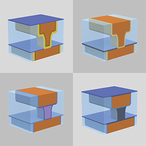
As one industry expert noted, however, it is increasingly difficult to further lower the k-value of these insulating films that separate the metal lines. One concept being explored is to replace dielectric films with air, which is a great insulator (k-value of 1.0). Various process flows to create these “airgaps” have been developed, such as the example below, and airgap structures have been shown to successfully reduce capacitance when introduced at higher metal levels.

Emerging Strategies Could Replace Current Technologies
Our industry experienced a significant technology inflection when interconnects switched from aluminum wires to copper in the late 1990s. Are similar big changes in our future? Some researchers are looking into alternate barrier materials. Copper interconnects must be completely enclosed by a barrier layer that blocks diffusion of copper into the surrounding material. Copper-manganese alloys for self-forming barriers, post-etch treatment films, and self-assembled monolayer barriers are some of the schemes being explored to enable continued interconnect scaling.
Another strategy under consideration is using cobalt as the bulk conductor material, replacing tungsten contacts and copper interconnects. Cobalt potentially has lower electrical resistance than tungsten in small contacts or local interconnects. Using cobalt, therefore, could enable devices that are faster or more power efficient. In addition, electromigration resistance, or ability to resist movement of atoms or ions during high current flow, is expected to be better for cobalt than for copper. A number of approaches are currently being explored for implementing cobalt deposition in production, including electrochemical plating, electroless plating, and CVD.

Cost-Effective Solutions Require Collaboration
Lastly, let’s not forget to consider the economics of the new materials and integration schemes that are being explored. Interconnect patterning is driving increases in cost and process complexity due to many multiple patterning steps at dense metal layers and vias. In order to advance the interconnect roadmap, cost-effective patterning solutions are needed. At the same time, resistance and capacitance need to be reduced without negatively impacting reliability. Meeting these technical and economic challenges requires greater collaboration across the ecosystem. By working together, equipment providers like Lam, chipmakers, circuit designers, and materials suppliers are enabling production of the ever more powerful devices that we have all come to expect from this extraordinary industry.